
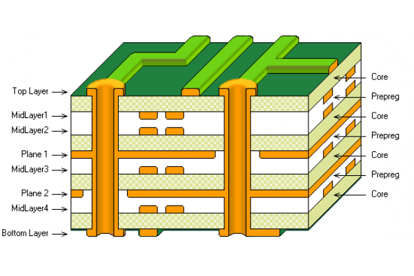
Layers Stack Up
A typical 4 Layer Stackup looks as follows
Signal 1
Ground
Power
Signal 2
Notice that the ground and power are interchangeable. If it
this PCB has many power islands AND there are controlled impedance traces, then
it may be a better idea to keep all the controlled impedance traces on Signal 1
and Ground layer beneath it. If controlled impedance traces refer the power
planes it must not either cross the split power plane junctions. If it is
unavoidable to pass the split power plane junctions, we should place stitching
capacitors.
The four layer trace has one inherent drawback. You can not
keep the power and ground traces tightly coupled for a typical 0.063” thick
PCB.
6 Layer stack up
A 4 layer stack up is pretty much straight forward. A 6 layer
stack up can have a number of variations. We should know the reasons behind
choice of these variations and select the one that suites our requirements. A
typical 6 Layer Stack up looks as follows.
Signal1
Ground
Signal2
Signal3
Power
Signal4
In this stack up the traces on signal2 and signal3 should be
routed in orthogonal fashion to avoid any potential cross talk. Care must be
taken not to route traces in parallel along signal 2 and signal 3.
All 4 signaling layers can refer to at least on power plane.
So all the four signaling layers can have controlled impedance traces. One
drawback of this arrangement is that the power and ground layers are not
adjacent. Adjacent power and ground planes provide inter plane capacitance
which is essential for providing low impedance path for the high frequency
power supply noise. With this in mind some engineers use the following stackup.
Signal1
Signal2
Ground
Power
Signal3
Signal4
The drawback of this stackup ? The Signal 1 and Signal 4 layers
do not refer to the power planes directly. This problem results in inability to
provide a controlled impedance on Signal 1 and Signal 4 layers.
So which stack up do you choose? If your design has very few
high speed signals that need controlled impedance routing, the second stack up
is better choice. You can route all the controlled impedance traces on Signal 2
and Signal 3 layers. The outer layers can be used for normal traces that do not
need controlled impedance.
If however, your design has large number of high speed traces
that need controlled impedance, the second stack up may not provide enough
room. In such case the first stack up is a better choice. If you happen to
choose the first stack up, try to fill the unused spaces on signal layers with
plane flooding. This will provide extra plane capacitance between the power and
ground layers required for the suppressing high frequency power supply noises.
A six layer stack up lacks the number of the power planes. A
typical microprocessor based system will need many small power islands, for
which a single power plane is not sufficient. In this scenario some of the
power islands will have to be on signal2 and/or power plane. If you find the
things hard you may use 8 Layer stack up.
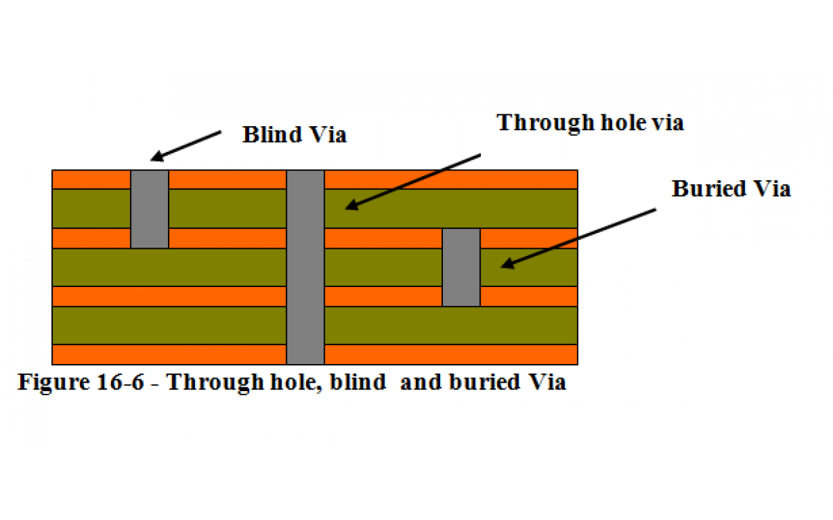
8 Layer stack up
A four layer or a 6 six layer stack have one or other
shortcoming. An 8 layer is the minimum number of layer that sufficiently
addresses all the signal integrity requirements. It does not mean that 4 layers
and 6 layers can not be used. The 4 layer and 8 layer can be and should be used
for lower cost. But they will not fulfill all the signal integrity and EMI
requirements is a dense PCB routing environment.
A typical 8 Layer Stackup looks as follows
Signal1
Ground
Signal2
Power
Ground
Signal3
Power
Signal4
The 8 Layer stack up provides ample routing space for
multiple power islands. In the above typical stack up all signaling layers have
at least one referencing power plane. The power and ground layer in the center
provides good inter plane capacitance. If your system has many power islands
and these power islands are next to the bottom layer, they do not have enough
power to ground capacitance. Also the return path for the high speed signals in
bottom layer (signal4) refer to the power plane which is not adjacent to a
ground plane. For these reasons, some engineers use an alternate stackup as
shown below.
Signal1
Ground
Power
Signal2
Signal3
Ground
Power
Signal4
By keeping the separation between signal2 and signal3 large
we can eliminate any potential crosstalk between signal2 and signal3.
A 4 layer stackup is pretty much straight forward. A 6 layer
stack up can have a number of variations. We should know the reasons behind
choice of these variations and select the one that suites our requirements.
Symmetry and Board Warping
In designing stackup, we should keep the it symmetrical with
respect to the copper and non copper planes. For example of second layer from
the top is a power or ground layer, then the second layer from the bottom
should also be a ground or a power layer. This requirement has to do more with
the mechanical requirement than the electrical requirement. An unsymmetrical
stack up will create warping during any process that applies heat the PCB. A
warped PCB will decrease yield especially if it has BGAs. The heights of the
solder balls will be different in a warped board leading to open conditions and
reducing yield. Keep your stack up symmetrical. If a power plane is partially
filled, fill up the remaining are with copper, even if they are not connected
to a net.


Aliquip veniam delectus, Marfa eiusmod Pinterest in do umami readymade swag. Selfies iPhone Kickstarter, drinking vinegar jean shorts fixie consequat flexitarian four loko.
Lorem ipsum dolor sit amet, justo aliquid reformidans ea vel, vim porro dictas et, ut elit partem invidunt vis. Saepe melius complectitur eum ea
Lorem ipsum dolor sit amet, justo aliquid reformidans ea vel, vim porro dictas et, ut elit partem invidunt vis. Saepe melius complectitur eum ea
Lorem ipsum dolor sit amet, justo aliquid reformidans ea vel, vim porro dictas et, ut elit partem invidunt vis. Saepe melius complectitur eum ea