Properties of the PCB
Each trace consists of a flat, narrow part of the copper foil that remains after etching. Its resistance, determined by its width, thickness, and length, must be sufficiently low for the current the conductor will carry. Power and ground traces may need to be wider than signal traces. In a multi-layer board one entire layer may be mostly solid copper to act as a ground plane for shielding and power return. For microwave circuits, transmission lines can be laid out in a planar form such as stripline or microstrip with carefully controlled dimensions to assure a consistent impedance. In radio-frequency and fast switching circuits the inductance and capacitance of the printed circuit board conductors become significant circuit elements, usually undesired; conversely, they can be used as a deliberate part of the circuit design, as in distributed element filters, antennae, and fuses, obviating the need for additional discrete components.
Materials
RoHS compliant PCB
The European Union bans the use of lead (among other heavy metals) in consumer items, a piece of legislature called the RoHS, for Restriction of Hazardous Substances, directive. PCBs to be sold in the EU must be RoHS-compliant, meaning that all manufacturing processes must not involve the use of lead, all solder used must be lead-free, and all components mounted on the board must be free of lead, mercury, cadmium, and other heavy metals.
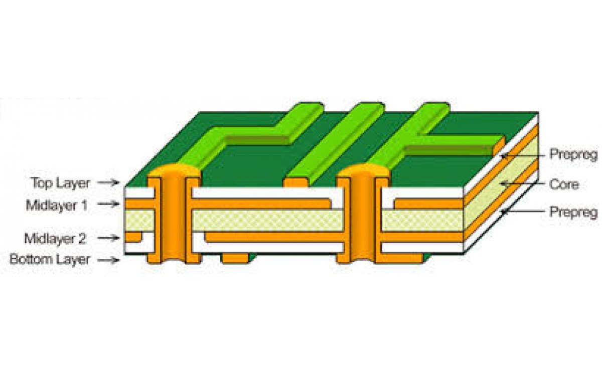
Laminates
Laminates are manufactured by curing under pressure and temperature layers of cloth or paper with thermoset resin to form an integral final piece of uniform thickness. The size can be up to 4 by 8 feet (1.2 by 2.4 m) in width and length. Varying cloth weaves (threads per inch or cm), cloth thickness, and resin percentage are used to achieve the desired final thickness and dielectric characteristics. Available standard laminate thickness are listed in ANSI/IPC-D-275.
The cloth or fiber material used, resin material, and the cloth to resin ratio determine the laminate's type designation (FR-4, CEM-1, G-10, etc.) and therefore the characteristics of the laminate produced. Important characteristics are the level to which the laminate is fire retardant, the dielectric constant(er), the loss factor (tδ), the tensile strength, the shear strength, the glass transition temperature (Tg), and the Z-axis expansion coefficient (how much the thickness changes with temperature).
There are quite a few different dielectrics that can be chosen to provide different insulating values depending on the requirements of the circuit. Some of these dielectrics are polytetrafluoroethylene (Teflon), FR-4, FR-1, CEM-1 or CEM-3. Well known pre-preg materials used in the PCB industry are FR-2(phenolic cotton paper), FR-3 (cotton paper and epoxy), FR-4 (woven glass and epoxy), FR-5 (woven glass and epoxy), FR-6 (matte glass and polyester), G-10 (woven glass and epoxy), CEM-1 (cotton paper and epoxy), CEM-2 (cotton paper and epoxy), CEM-3 (non-woven glass and epoxy), CEM-4 (woven glass and epoxy), CEM-5 (woven glass and polyester). Thermal expansion is an important consideration especially with ball grid array (BGA) and naked die technologies, and glass fiber offers the best dimensional stability.
FR-4 is by far the most common material used today. The board stock with unetched copper on it is called "copper-clad laminate".
With decreasing size of board features and increasing frequencies, small nonhomogeneities like uneven distribution of fiberglass or other filler, thickness variations, and bubbles in the resin matrix, and the associated local variations in the dielectric constant, are gaining importance.
Key substrate parameters
The circuitboard substrates are usually dielectric composite materials. The composites contain a matrix (usually an epoxy resin) and a reinforcement (usually a woven, sometimes nonwoven, glass fibers, sometimes even paper), and in some cases a filler is added to the resin (e.g. ceramics; titanate ceramics can be used to increase the dielectric constant).
The reinforcement type defines two major classes of materials: woven and non-woven. Woven reinforcements are cheaper, but the high dielectric constant of glass may not be favorable for many higher-frequency applications. The spatially nonhomogeneous structure also introduces local variations in electrical parameters, due to different resin/glass ratio at different areas of the weave pattern. Nonwoven reinforcements, or materials with low or no reinforcement, are more expensive but more suitable for some RF/analog applications.
The substrates are characterized by several key parameters, chiefly thermomechanical (glass transition temperature, tensile strength, shear strength, thermal expansion), electrical (dielectric constant, loss tangent, dielectric breakdown voltage, leakage current, tracking resistance...), and others (e.g. moisture absorption).
At the glass transition temperature the resin in the composite softens and significantly increases thermal expansion; exceeding Tg then exerts mechanical overload on the board components - e.g. the joints and the vias. Below Tg the thermal expansion of the resin roughly matches copper and glass, above it gets significantly higher. As the reinforcement and copper confine the board along the plane, virtually all volume expansion projects to the thickness and stresses the plated-through holes. Repeated soldering or other exposition to higher temperatures can cause failure of the plating, especially with thicker boards; thick boards therefore require a matrix with a high Tg.
The materials used determine the substrate's dielectric constant. This constant is also dependent on frequency, usually decreasing with frequency. As this constant determines the signal propagation speed, frequency dependence introduces phase distortion in wideband applications; as flat a dielectric constant vs frequency characteristics as is achievable is important here. The impedance of transmission lines decreases with frequency, therefore faster edges of signals reflect more than slower ones.
Dielectric breakdown voltage determines the maximum voltage gradient the material can be subjected to before suffering a breakdown (conduction, or arcing, through the dielectric).
Tracking resistance determines how the material resists high voltage electrical discharges creeping over the board surface.
Loss tangent determines how much of the electromagnetic energy from the signals in the conductors is absorbed in the board material. This factor is important for high frequencies. Low-loss materials are more expensive. Choosing unnecessarily low-loss material is a common engineering error in high-frequency digital design; it increases the cost of the boards without a corresponding benefit. Signal degradation by loss tangent and dielectric constant can be easily assessed by an eye pattern.
Moisture absorption occurs when the material is exposed to high humidity or water. Both the resin and the reinforcement may absorb water; water also may be soaked by capillary forces through voids in the materials and along the reinforcement. Epoxies of the FR-4 materials aren't too susceptible, with absorption of only 0.15%. Teflon has very low absorption of 0.01%. Polyimides and cyanate esters, on the other side, suffer from high water absorption. Absorbed water can lead to significant degradation of key parameters; it impairs tracking resistance, breakdown voltage, and dielectric parameters. Relative dielectric constant of water is about 73, compared to about 4 for common circuit board materials. Absorbed moisture can also vaporize on heating, as during soldering, and cause cracking and delamination, the same effect responsible for "popcorning" damage on wet packaging of electronic parts. Careful baking of the substrates may be required to dry them prior to soldering.
Common substrates
Often encountered materials:
- FR-2, phenolic paper or phenolic cotton paper, paper impregnated with a phenol formaldehyde resin. Common in consumer electronics with single-sided boards. Electrical properties inferior to FR-4. Poor arc resistance. Generally rated to 105 °C.
- FR-4, a woven fiberglass cloth impregnated with an epoxy resin. Low water absorption (up to about 0.15%), good insulation properties, good arc resistance. Very common. Several grades with somewhat different properties are available. Typically rated to 130 °C.
- Aluminum, or metal core board or insulated metal substrate (IMS), clad with thermally conductive thin dielectric - used for parts requiring significant cooling - power switches, LEDs. Consists of usually single, sometimes double layer thin circuit board based on e.g. FR-4, laminated on aluminum sheet metal, commonly 0.8, 1, 1.5, 2 or 3 mm thick. The thicker laminates sometimes also come with thicker copper metalization.
- Flexible substrates - can be a standalone copper-clad foil or can be laminated to a thin stiffener, e.g. 50-130 µm
- Kapton or UPILEX,a polyimide foil. Used for flexible printed circuits, in this form common in small form-factor consumer electronics or for flexible interconnects. Resistant to high temperatures.
- Pyralux, a polyimide-fluoropolymer composite foil. Copper layer can delaminate during soldering.
Less-often encountered materials:
- FR-1, like FR-2, typically specified to 105 °C, some grades rated to 130 °C. Room-temperature punchable. Similar to cardboard. Poor moisture resistance. Low arc resistance.
- FR-3, cotton paper impregnated with epoxy. Typically rated to 105 °C.
- FR-5, woven fiberglass and epoxy, high strength at higher temperatures, typically specified to 170 °C.
- FR-6, matte glass and polyester
- G-10, woven glass and epoxy - high insulation resistance, low moisture absorption, very high bond strength. Typically rated to 130 °C.
- G-11, woven glass and epoxy - high resistance to solvents, high flexural strength retention at high temperatures.Typically rated to 170 °C.
- CEM-1, cotton paper and epoxy
- CEM-2, cotton paper and epoxy
- CEM-3, non-woven glass and epoxy
- CEM-4, woven glass and epoxy
- CEM-5, woven glass and polyester
- PTFE, ("Teflon") - expensive, low dielectric loss, for high frequency applications, very low moisture absorption (0.01%), mechanically soft. Difficult to laminate, rarely used in multilayer applications.
- PTFE, ceramic filled - expensive, low dielectric loss, for high frequency applications. Varying ceramics/PTFE ratio allows adjusting dielectric constant and thermal expansion.
- RF-35, fiberglass-reinforced ceramics-filled PTFE. Relatively less expensive, good mechanical properties, good high-frequency properties.
- Alumina, a ceramic. Hard, brittle, very expensive, very high performance, good thermal conductivity.
- Polyimide, a high-temperature polymer. Expensive, high-performance. Higher water absorption (0.4%). Can be used from cryogenic temperatures to over 260 °C.
Copper thickness
Copper thickness of PCBs can be specified directly or as the weight of copper per area (in ounce per square foot) which is easier to measure. One ounceper square foot is 1.344 mils or 34 micrometers thickness. Heavy copper is a layer exceeding three ounces of copper per ft2, or approximately 0.0042 inches (4.2 mils, 105 μm) thick. Heavy copper layers are used for high current or to help dissipate heat.
On the common FR-4 substrates, 1 oz copper per ft2 (35 µm) is the most common thickness; 2 oz (70 µm) and 0.5 oz (18 µm) thickness is often an option. Less common are 12 and 105 µm, 9 µm is sometimes available on some substrates. Flexible substrates typically have thinner metalization. Metal-core boards for high power devices commonly use thicker copper; 35 µm is usual but also 140 and 400 µm can be encountered.